Optically Controlled Attenuator
Along with Dr. Edward Tong (of the SMA receiver lab SAO), I have designed, fabricated and measured a WR3.4 optically controlled waveguide modulator. The symmetric device consists of offset input and output waveguides connected by an E-plane-mounted 25μm thick silicon chip. Patterned on the chip is a pair of radial stub waveguide probes connected by a 1mm long section of microstrip transmission line. The waveguide probes have been optimized in Ansys HFSS to provide return losses of better than -25 dB from 220GHz to 330GHz. Illumination of the chip at photon energies larger than the silicon bandgap generates free charge carriers in the silicon substrate, modulating its conductivity and dielectric constant. This photoconductive effect allows for the modulation of the millimeter-wave loss along the microstrip transmission line. Measurements of the device have been made using a custom built 1-port reflectometer in WR3.4 waveguide. Two-port s-paramters are extracted using a two standard/two reference plance calbration scheme. An inexpensive 805nm multimode laser diode driven by a voltage controlled current source was used for illumination.
The modulation bandwidth of this device was measured to be 2.07MHz at moderate modulation depths, consistent with carrier lifetime calculations. The modulation bandwidth was measured by observing the carrier to sideband ratio of the down-converted received signal on a spectrum analyzer. Ultimately, the bandwidth of such a device should be limited by the minority carrier lifetime in the silicon substrate. Efforts to measure the modulation bandwidth with a purpose-built fast optical source are underway.
At low modulation frequency, the device operates as a continuously variable attenuator. Compared to optically-controlled dielectric-loaded waveguide attenuators, the increased millimeter-wave power density in microstrip transmission line and focused optical illumination allows our device to achieve a reasonably wide dynamic range with modest optical powers. At an incident optical power of 500mW, we have demonstrated up to 45dB of attenuation. With no illumination, the device exhibits an insertion loss between 1dB and 1.5dB, partially due to loss in the flange matings and input and output waveguide transmission loss. The measured attenuation varies linearly and slowly with frequency and is a smooth monotonically increasing function of incident optical power. Such properties make this device an ideal candidate for use in conjunction with a directional coupler as a source leveling-loop or a DC-stabilized modulator or 'chopper'. These applications may find use in varied areas such as millimeter wave antenna mapping or millimeter-wave vector network analyzer extenders.
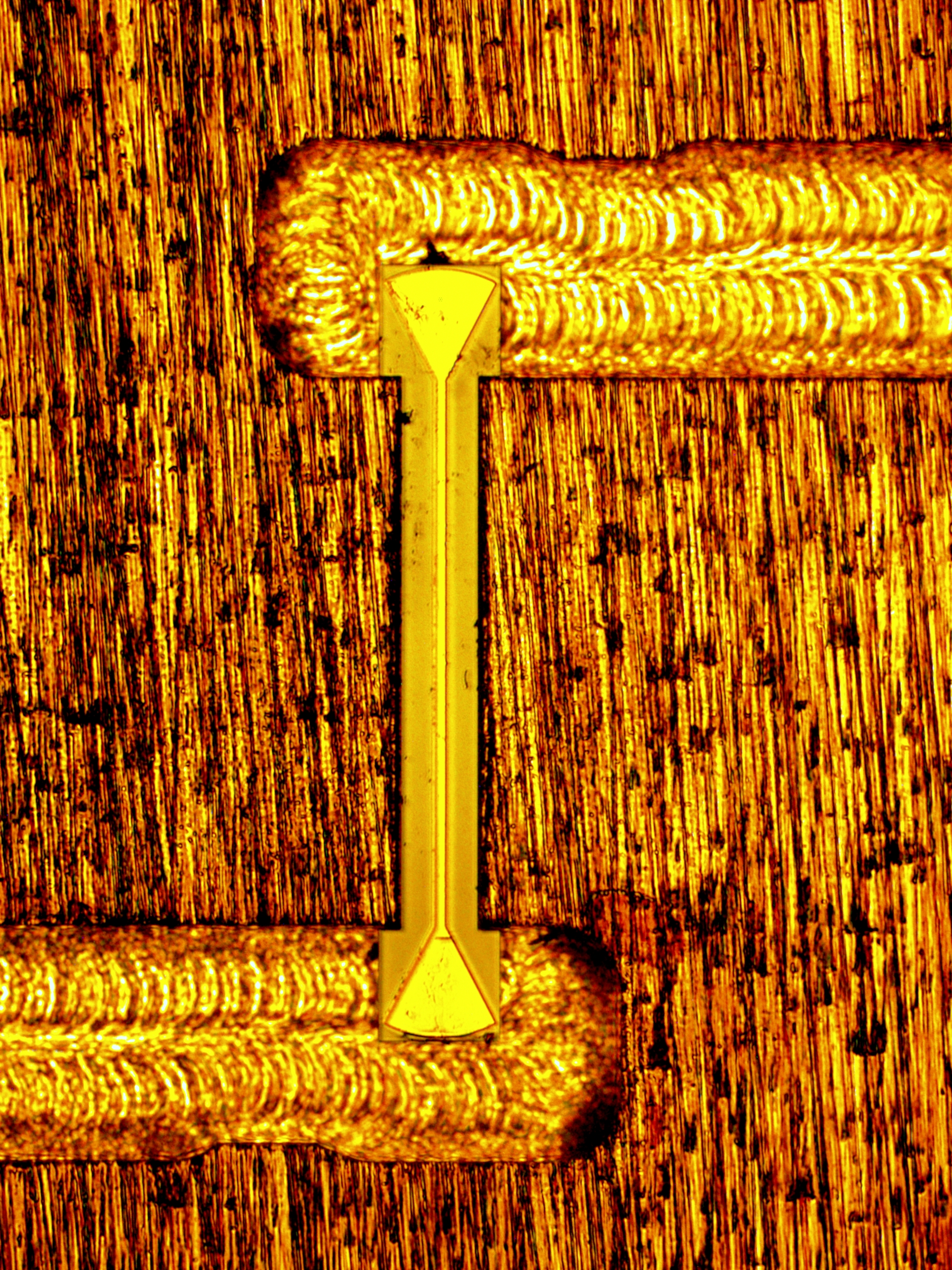
A view of the microstrip-to-waveguide probe chip as installed in the E-plane split block. Also visible are the WR3.4 waveguides each with a single capacitive tuning step.
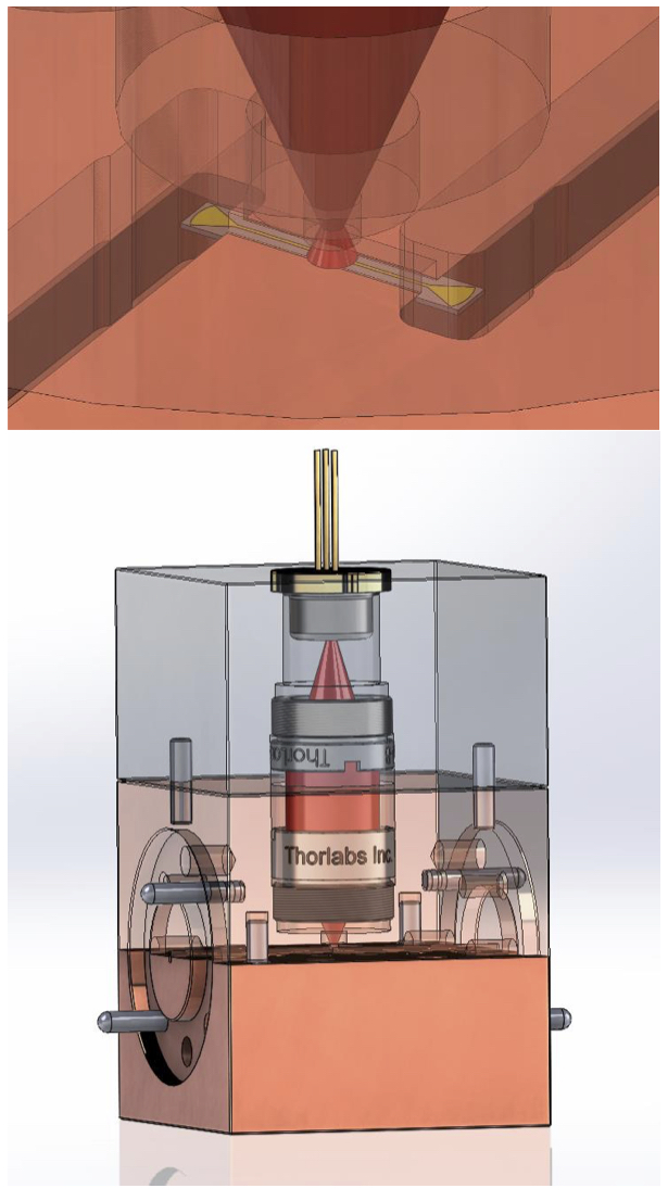
(Top) View of probe chip as assembled in the waveguide block. Light passes through a small hole in the upper cavity onto the chip. (Bottom) Completed assembly of waveguide split-block and laser diode block. Shown in red is the beam of the 808nm laser diode as collimated and focused by the two-lens system.
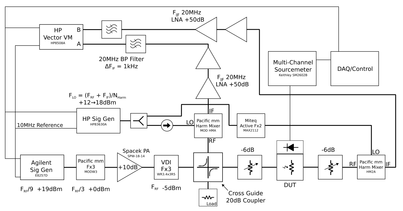
Schematic of transmission measurement scheme. A coupled portion of the RF signal and the remainder after passing through the DUT are sent through a down-converting and amplification chain to an HP8508A Vector Voltmeter for measurement of the relative amplitude and phase of the transmitted signal.
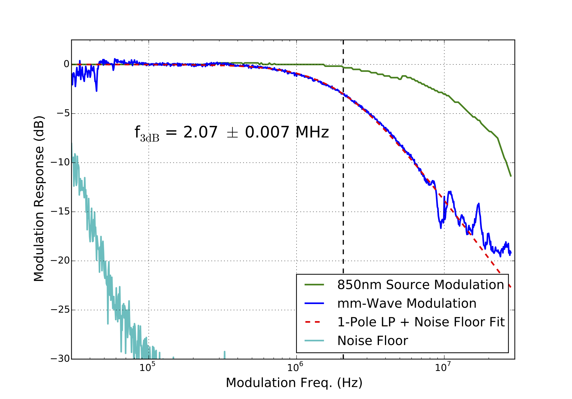
Measurement of the modulation bandwidth of the device using a 20MHz 5mW IR LED source. A 3dB bandwidth of more than 2MHz is measured corresponding to a ~77ns carrier lifetime.